12.5.1 The Watson Virtual Machine revisited
Chapter 11 introduced the Watson Virtual Machine. This machine, illustrated in Figure 11.1, consists of a main memory, CPU and data bus. A somewhat more detailed view of the machine is given in Figure 12.32.
The main memory of the Watson VM is composed of 256 words, each 16 bits wide. While not discussed in Chapter 11, Figure 12.32 shows that the interface to main memory (RAM) consists of two registers, the memory address register (MAD) and the memory data register (MDR). During both “read” and “write” operations, the MAR is used to hold the address of the memory location to be accessed. Since there are 256 words of memory in the Watson VM, numbered 0 – 255, the MAR is eight bits wide, enabling it to hold addresses in the range 0000 0000two to 1111 1111two (0 – 255). During “write” operations, the 16-bit value to be written into memory will be placed in the MDR. During “read” operations the value of the memory location to be read will be output to the MDR. Thus, the memory data register can function both in an input role (for “write” operations) and in an output role (for “read” operations). The memory address register, on the other hand, always functions in an input role – specifying the location to be accessed.
The majority of Figure 12.32 concerns itself with the details of the Watson Virtual Machine CPU. Special emphasis is given to illustrating the major control and data lines interconnecting the various components.
In Figure 11.1 the CPU is shown as consisting of four components: a program counter, an instruction register, a collection of sixteen general-purpose registers, and four status bits. An examination of Figure 12.32 reveals that in addition to these components, there are four additional components labeled “control logic”, “ALU”, “MUX”, and “decoder”.
As discussed in Chapter 11, the behavior of a computer at the machine level can be understood in terms of the five-stage instruction cycle:
-
Fetch the next instruction from memory
-
Increment the program counter
-
Decode the current instruction
-
Execute the current instruction
-
Return to step 1.
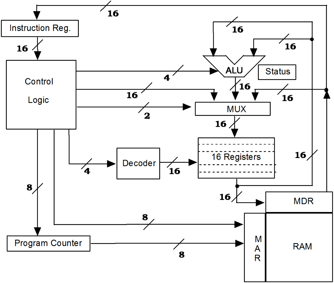
Figure 12.32: The Watson Virtual Machine (detailed view)
The control logic, or control unit, is the component of the Watson VM responsible for implementing the instruction cycle. It does so by generating the signals necessary to direct the other components of the machine to carry out their tasks in an orderly manner. For this reason, the control unit is sometimes referred to as the “traffic cop” of the CPU. Input to the control unit is from the instruction register, since it must have access to the bit pattern that represents the instruction for it to do its job. Because of the central role played by the control unit, its outputs are connected by various data and signal lines to most of the other components of the machine.
The ALU (Arithmetic / Logic Unit) is responsible for the math and logic operations performed by the machine. If the control unit is the “traffic cop”, then the ALU is the “calculator”, responsible for performing addition, subtraction, and the various logic operations. The ALU of the Watson VM receives two 16-bit input values from the general-purpose registers and one 4-bit control code from the control unit. The 16-bit values represent the operands. The control code, derived from the op-code of the current instruction, specifies which arithmetic or logic operation is to be performed on those operands. Output from the ALU is directed to a multiplexer that is responsible for routing data to the general-purpose registers. This makes sense, because the results of arithmetic and logic operations must end up in one of the registers.
Taking a closer look at the multiplexer, we see that it has three 16-bit data inputs, one from the control unit, one from the ALU and one from the memory data register. There is also a two-bit selector signal sent from the control unit to the multiplexer in order to tell it which input data values should be passed on.
The reason for the three data inputs into the multiplexer has to do with the sources that can generate register values. Arithmetic and logic instructions, like ADD , require that the registers be able to receive input from the ALU in order to place the result of the operation into the destination register. LOAD instructions require that registers be able to receive data from main memory. The LOADIMM instruction requires that “immediate” values, which are part of the instruction and thus located in the instruction register, be loaded into registers. The two-bit selector signal, under the direction of the control unit, specifies which of these three sources should be routed to the registers.
Building this multiplexer is a straightforward exercise – we simply arrange sixteen of the four-input multiplexers of Figure 12.19 in parallel. The reason for using four-input multiplexers, even though we only have three input sources, is that multiplexers only come in powers of two – two input, four input, eight input, etc. Thus one of the inputs on each of the sixteen standard four-input multiplexers will be unused. While this is may seem a tad wasteful, it won’t cause any operational difficulties.
The reason for needing sixteen copies of the “standard” four-input multiplexers is that our data values are sixteen bits wide. Thus, each of the “standard” four-input multiplexers will pass only one bit of the 16-bit data value to an output line. By arranging sixteen of these “one-bit wide” multiplexers in parallel, we can build a multiplexer capable of routing all 16 bits of the selected data value simultaneously.
The final component of the CPU we’ll look at is the four-input decoder, located between the control unit and the bank of general-purpose registers. The task of this decoder is to select one of the sixteen registers for access – either for receiving a value from the MUX, or for sending a register value to either main memory or the ALU. This decoder would be similar to the three-to-eight decoder of Figure 12.16, but extended to handle four input lines and sixteen output lines.
In addition to the memory and CPU, the Watson VM also contains a data bus. This bus was illustrated in Figure 11.1 simply as a path connecting the CPU and memory. In Figure 12.32 the representation of the data bus is much more detailed. It is presented as a number of separate data and address lines that connect components of the CPU to the RAM. In the figure, there are two sets of 8-bit address lines, both leading into the memory address register (MAR). There are also two sets of 16-bit data lines connected to the memory data register (MAD), one set for input and one set for output.
The memory location to be retrieved, and thus the address to be loaded into the memory address register can originate from two separate CPU components, the control unit or the program counter. The address comes from the program counter when the machine is fetching the next instruction from memory. The address comes from the control unit when the machine is fetching an operand, such as a variable, from memory.
The input data lines leading to the memory data register originate from the block of sixteen general-purpose registers. This makes sense, since in order to store a value into memory, the value must first be in a register.
Looking at the output data lines originating from the memory data register, we see that a 16-bit memory value can be transferred to either the instruction register or the multiplexer that routes values to the general-purpose registers. If the machine is performing an instruction fetch, the bit pattern being retrieved from memory represents an instruction and therefor must be sent to the instruction register. If the machine is in the process of fetching an operand, that operand should end up in one of the sixteen general-purpose registers and is thus sent to the multiplexer.
The remainder of this section presents circuit-level designs for a simple ALU and memory. Even though the Watson VM is a very simple microcomputer by today’s standards, it is still much too complex for us to go through a full design of its components. Instead, the components we will look at will be even simpler. Their development, however, should convince you that computers can be constructed from the combinational and sequential circuits of section 12.3 and 12.4.